
High-Performance Nanomaterials & Organic Frameworks
Explore our core commercial catalog, optimized for high thermal stability, selective gas adsorption, and electrical conductivity.
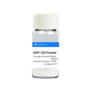
Best MOF-303 Powder Metal Organic Frameworks (MOFs) from China Suppliers Factory
View Product Details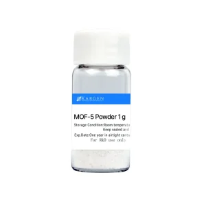
Best MOF-5 Powder Metal Organic Frameworks for Gas Storage Solutions
View Product Details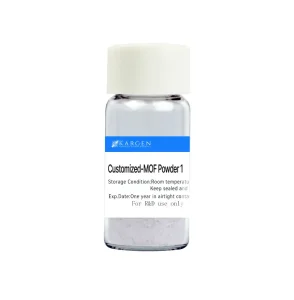
High-Quality Customized Metal Organic Frameworks (MOFs) Tailored Solutions
View Product Details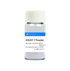
High-Performance KAUST-7 MOFs for CO2 Adsorption & Chemical Stability
View Product Details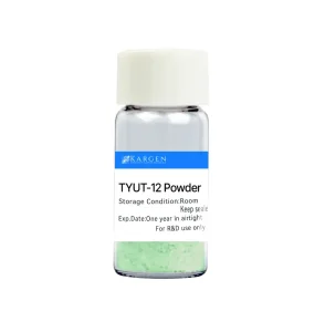
High-Quality TYUT-12 Powder Metal Organic Frameworks Adsorption Factory
View Product Details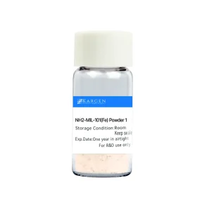
Best NH2-MIL-101(Fe) Powder for Advanced Catalysis and Sensing Applications
View Product Details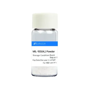
High-Quality MIL-100(Al) Powder Metal Organic Frameworks Exporters
View Product Details
High-Quality China MOF-5 Powder Factory for Gas Storage & Pollutant Removal
View Product DetailsSynthesis Engineering & Material Physics of Copper Nanoparticles
An authoritative technical evaluation of copper nanoparticle morphology, surface passivation kinetics, and electrical transport mechanisms in industrial environments.
Morphology & Particle Size Control
Copper nanoparticles (CuNPs) exhibit profound quantum size effects when engineered within the 10nm to 100nm regime. Chemical reduction pathways utilize precise polyol methods and surfactant capping (e.g., Polyvinylpyrrolidone / PVP) to achieve spherical, nanowire, or core-shell architectures with ultra-narrow size distribution metrics ($d_{50} \le 25\text{ nm}$).
Anti-Oxidation Passivation Kinetics
Unprotected elemental copper rapidly oxidizes to $\text{Cu}_2\text{O}$ and $\text{CuO}$ upon atmospheric exposure. Advanced manufacturing employs inline atomic layer passivation, organic self-assembled monolayers (SAMs), or silver shell cladding ($\text{Cu}@\text{Ag}$) to suppress oxygen diffusion while preserving intrinsic electrical conductivity up to $250^\circ\text{C}$.
Electrical & Thermal Transport Dynamics
CuNPs deliver high bulk thermal conductivity ($398\text{ W/m}\cdot\text{K}$) and near-precious-metal electrical resistivity ($1.68 \times 10^{-8}\ \Omega\cdot\text{m}$). Low-temperature sintering kinetics allow neck formation between particles at $140^\circ\text{C}-180^\circ\text{C}$, enabling compatibility with heat-sensitive flexible polymer substrates.
| Material Benchmark Parameter | High-Purity CuNPs (Our Grade) | Silver Nanoparticles (AgNPs) | Gold Nanoparticles (AuNPs) | Standard Micron Copper Powder |
|---|---|---|---|---|
| Mean Particle Size ($d_{50}$) | 10 nm – 80 nm (Customizable) | 20 nm – 100 nm | 5 nm – 50 nm | 1.0 µm – 10.0 µm |
| Raw Material Unit Cost Index | Economical (1x Base) | High (15x – 25x) | Ultra-High (500x+) | Very Low (0.4x) |
| Sintering Threshold Temp. | 140°C – 180°C | 130°C – 160°C | 150°C – 200°C | > 650°C |
| Thermal Conductivity (W/m·K) | ~380 – 395 | ~415 – 425 | ~310 – 315 | ~320 (Porous) |
| Dispersibility & Ink Stability | High (Surfactant Capped) | High | High | Low (Rapid Settling) |
Information Gain: Overcoming the Sintering-Oxidation Paradox
Conventional conductive metallic inks reliance on silver introduces prohibitive cost scaling for mass electronics manufacturing. Our proprietary chemical reduction process integrates a dual-stage oleic acid and organosilane surface matrix. This engineering milestone effectively delays the thermodynamic onset of copper oxidation up to 180 days under ambient storage while maintaining instantaneous micro-pulse photonic sintering compatibility.
China Supply Chain Dominance & Ton-Scale Production Infrastructure
Leveraging direct upstream metal refining integration, advanced mechanochemical scale-up systems, and stringent ISO quality controls.
Upstream Raw Material Integration
Situated within China's primary non-ferrous metallurgical cluster, our plant secures continuous access to ultra-pure electrolytic copper cathode feedstock. This vertical integration eliminates intermediate trading markups, ensuring stable pricing and uninterrupted bulk production even during global raw material fluctuations.
Continuous Wet-Chemical Synthesis
Moving away from legacy batch-by-batch reaction kettles, our factory utilizes automated micro-fluidic continuous flow reactors. This setup ensures real-time temperature, mixing rate, and pH monitoring, driving batch-to-batch coefficient of variation (CV) down to less than 2.5%.
Rigorously Validated QC Protocols
Every commercial production batch undergoes comprehensive diagnostic evaluation: Transmission Electron Microscopy (TEM) for size verification, X-Ray Diffraction (XRD) for phase purity, Inductively Coupled Plasma Mass Spectrometry (ICP-MS) for elemental purity, and Thermogravimetric Analysis (TGA) for capping shell verification.
Tailored Engineering for Global Industrial Buyers
From custom surface chemistry functionalization to specialized non-polar dispersion solvents and international vacuum cold-chain packaging.
1. Surface Capping & Ligand Exchange
We provide tailor-made surface modification to match your specific solvent matrix:
- PVP / Polyvinylpyrrolidone: Hydrophilic, polar solvent compatible (Water, Ethanol, Isopropanol).
- Oleic Acid / Oleylamine: Hydrophobic, non-polar solvent dispersion (Toluene, Hexane, Terpineol).
- Citrate-Stabilized: Biocompatible formulation for medical and sensor applications.
- Conductive Polymer Shells: PEDOT:PSS coating for enhanced low-temp electronic percolation.
2. Ready-to-Use Liquid Dispersions
To prevent airborne powder handling and aggregation, we deliver pre-dispersed nano-slurries:
- Solid loading concentrations from 10 wt% up to 70 wt%.
- Zero-settling anti-sedimentation additives for long shelf-life.
- Viscosity tuning from low-viscosity inkjet printing (5-15 cP) to high-viscosity screen printing pastes (>50,000 cP).
3. Protective Packaging & Logistics
Copper nanoparticles require stringent packaging safeguards to prevent atmospheric oxidation during transit:
- Hermetically sealed multi-layer aluminum-foil vacuum bags with inert Argon gas purge.
- Cold-chain temperature-controlled international shipping options.
- Available package sizes: 100g sample containers, 1kg foil bags, 25kg industrial drums, to ton-drum shipping.
Key Industry Trends & Technological Drivers (2025 – 2032)
Examining the global industrial transition toward copper nanomaterials in energy transition, flexible electronics, and green chemistry.
1. Flexible Printed Electronics & 3D Circuits
The global printed electronics market demands conductive inks compatible with heat-sensitive substrates like PET, PI, and paper. Low-sintering copper nanoparticles enable high-speed reel-to-reel inkjet and flexographic printing of RFID tags, smart packaging, wearable biomedical sensors, and micro-heaters at a fraction of silver ink costs.
2. MLCC Inner Electrode Material Substitution
Multi-Layer Ceramic Capacitors (MLCCs) used in 5G smartphones and Electric Vehicles (EVs) are downsizing rapidly. Ultrafine 20-50nm copper nanoparticles are replacing nickel and micron-copper pastes in inner electrode terminal layers to achieve higher capacitance density without dielectric breakdown risk during high-temperature co-firing.
3. Electro-Catalytic CO2 Reduction & Green Chemistry
Copper nanomaterials possess unique surface binding affinities for C-C coupling intermediate species. Oxide-derived copper nanoparticles ($\text{OD-Cu}$) act as highly selective catalysts in industrial electrochemical systems converting captured $\text{CO}_2$ into valuable ethylene, ethanol, and green hydrocarbon chemical feedstocks.
4. Next-Gen Antimicrobial & Marine Antifouling
Due to continuous release of $\text{Cu}^{2+}$ ions, sub-50nm copper nanoparticles exhibit broad-spectrum antimicrobial, antiviral, and anti-fungal efficacy. They are increasingly integrated into medical textiles, HVAC HEPA filters, self-sterilizing touch surfaces, and eco-friendly marine antifouling hull coatings replacing toxic organotin additives.
Localized High-Value Application Scenarios
Discover how lead enterprise clients integrate our copper nanoparticles across critical engineering verticals.
Automotive EV Thermal Interface Materials (TIMs)
Challenge: Electric vehicle battery packs and silicon carbide (SiC) power inverters require ultra-high heat dissipation to prevent thermal runaway.
Solution: Incorporating 40nm CuNPs into silicone and epoxy thermal pastes raises bulk thermal conductivity beyond $12\text{ W/m}\cdot\text{K}$ while maintaining low viscosity for micro-gap pump-out resistance.
High-Density Interconnect (HDI) PCB Metallization
Challenge: Laser micro-vias in ultra-thin circuit boards require reliable void-free copper plating.
Solution: Formulating specialized CuNP seed suspensions provides uniform chemical adsorption on via walls, speeding up subsequent electroplating deposition and eliminating micro-void failures under thermal cycling tests.
Solar Cell Metallization Pastes (Photovoltaics)
Challenge: High silver prices compromise profitability for HJT and TOPCon solar cell grid finger lines.
Solution: Our silver-coated copper nanoparticles ($\text{Cu}@\text{Ag}$) replace up to 50% of silver powder in front-side screen printing pastes without compromising cell efficiency or long-term damp-heat reliability ($85^\circ\text{C} / 85\%\text{ RH}$).
Global Regulatory Authorization & Regional Service Centers
Ensuring complete compliance with international chemical safety standards and seamless import customs clearance.
Full EU REACH & RoHS Compliance
Our copper nanoparticles fully comply with European Chemical Agency (ECHA) REACH registration requirements, TSCA (USA), and RoHS Directive 2011/65/EU. Heavy metal impurities (Lead, Cadmium, Mercury, Hexavalent Chromium) are guaranteed below strictly enforced parts-per-million (PPM) thresholds.
Standardized Safety Documentation
Every shipment is dispatched with batch-specific Certificates of Analysis (COA), 16-section Safety Data Sheets (SDS / MSDS) compliant with GHS Revision 8, and detailed handling guidelines for safe laboratory and industrial mixing practices.
Localized Field Application Support
Our dedicated material science support staff provides direct engineering assistance across North America, Europe, and Asia-Pacific. From dispersion troubleshooting to ink formulation and sintering protocol optimization, our PhD technical team responds within 24 business hours.
Frequently Asked Technical Questions
Addressing core procurement, technical evaluation, and handling questions from industrial engineers.
How do you prevent copper nanoparticles from oxidizing during long-term storage?
We utilize a multi-tier anti-oxidation protective framework. First, during chemical synthesis, nanoparticles are passivated with a surface-capping shell of PVP, oleic acid, or silver coating ($\text{Cu}@\text{Ag}$). Second, materials are vacuum-packaged under an ultra-pure Argon or Nitrogen blanket inside multi-layer aluminum barrier bags. When stored in a cool, dry environment ($<25^\circ\text{C}$), our dry powders and dispersions retain chemical purity for 12 months.
What is the minimum sintering temperature for your copper nanoparticle ink grades?
Our ultra-fine $20\text{ nm}$ spherical copper nanoparticle grades initiate necking and inter-particle sintering at temperatures as low as $140^\circ\text{C}$ in inert/reducing atmosphere ($\text{N}_2 / \text{H}_2$ or Formic Acid vapor). For ambient air sintering, we recommend photonic sintering (intense pulsed light / IPL) or laser curing, which sinters the conductive layer in milliseconds without thermal damage to substrate films like PET or Paper.
Can I order custom particle sizes and specific solvent dispersions?
Yes. As an OEM manufacturer, we produce targeted mean diameters from $10\text{ nm}$ up to $100\text{ nm}$ with tight tolerances. We offer custom liquid dispersions in Deionized Water, Ethanol, Isopropanol, Terpineol, Toluene, or customer-supplied solvent systems with solid loading content ranging from 10 wt% to 70 wt%.
What are the pricing benefits of Copper Nanoparticles compared to Silver Nanoparticles?
Copper raw material costs are less than 1/100th that of metallic silver. Even when accounting for precision nanostructure synthesis and anti-oxidation capping processing, our high-conductivity copper nanoparticle pastes and inks achieve a 50% to 70% total cost saving over equivalent silver-based formulations, making mass commercialization viable for printed electronics and solar metallization.
What testing documentation is included with sample evaluation orders?
All evaluation samples are dispatched with a detailed Certificate of Analysis (COA) containing TEM particle morphology micrographs, Dynamic Light Scattering (DLS) size distribution curves, X-Ray Diffraction (XRD) phase spectrum confirming zero oxide contamination, ICP-MS chemical purity data, and a 16-section SDS sheet.
What is your typical lead time for ton-scale bulk procurement orders?
Standard product evaluation samples (100g – 1kg) are dispatched within 3 business days via express air courier. Commercial bulk production orders (100kg to Ton-scale) carry a standard manufacturing cycle of 10 to 14 calendar days, supported by expedited sea or air freight handling through our logistics network.
Advanced Material Formulations & Specialty Frameworks
Browse the second suite of specialized nanomaterials, high-adsorption framework structures, and industrial catalyst powders.
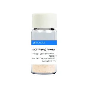
High-Quality MOF-74(Mg) Powder for Enhanced Gas Adsorption
View Product Details
High-Quality China MOF-303 Powder Factory for Gas Separation
View Product Details
High-Quality KAUST-7 MOFs: High Stability CO2 Adsorption Solutions
View Product Details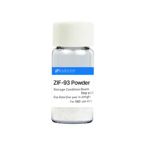
Best ZIF-93 Powder Metal Organic Frameworks (MOFs) Supplier
View Product Details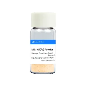
Best China Factory: MIL-101(Fe) Powder MOFs for Adsorption & Catalysis
View Product Details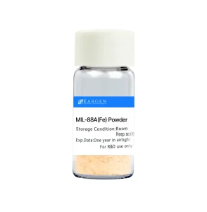
Best MIL-88A(Fe) Powder MOFs for Environmental Remediation
View Product Details
High-Quality China MOF-303 Suppliers for Gas & Liquid Separation
View Product Details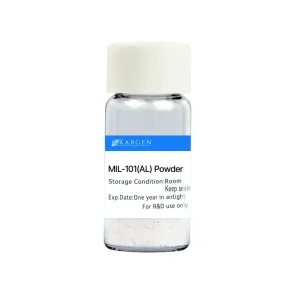
Best China MIL-101(Al) Powder Metal Organic Frameworks Exporter
View Product DetailsAccelerate Your Advanced Material Development
Request free evaluation samples (100g), custom solvent dispersion trials, or technical white paper documentation directly from our R&D engineering team.